After Hours Shipping

Real Time Order Tracking

Flexible Delivery Options

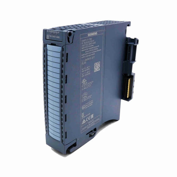
| General information | S7-1500, DQ 16x24V DC/0.5A HF | S7-1500, DQ 32x24VDC/0.5A HF | S7-1500, DQ 8x24VDC/2A HF | S7-1500, DQ 16×24…48VUC/125VDC/0.5A ST |
| Product type designation | DQ 16x24VDC/0.5A HF | DQ 32x24VDC/0.5A HF | DQ 8x24VDC/2A HF | DQ 16×24 … 48 V UC/125 V DC/0.5 A ST |
| HW functional status | From FS02 | From FS02 | FS03 | FS02 |
| Firmware version | V1.1.0 | V1.1.0 | V2.2.0 | V1.0.0 |
| ·
● FW update possible · |
Yes | Yes | Yes | |
| Product function | ||||
| ·
● I&M data · |
Yes; I&M0 to I&M3 | Yes; I&M0 to I&M3 | Yes; I&M0 to I&M3 | Yes; I&M0 to I&M3 |
| ·
● Isochronous mode · |
Yes | Yes | No | No |
| ·
● Prioritized startup · |
Yes | Yes | Yes | Yes |
| Engineering with | ||||
| ·
● STEP 7 TIA Portal configurable/integrated from version · |
V13 SP1 / – | V13 SP1 / – | V13 SP1 / – | V13 SP1 / – |
| ·
● STEP 7 configurable/integrated from version · |
V5.5 SP3 / – | V5.5 SP3 / – | ||
| ·
● PROFIBUS from GSD version/GSD revision · |
V1.0 / V5.1 | V1.0 / V5.1 | V1.0 / V5.1 | V1.0 / V5.1 |
| ·
● PROFINET from GSD version/GSD revision · |
V2.3 / – | V2.3 / – | V2.3 / – | V2.3 / – |
| Operating mode | ||||
| ·
● DQ · |
Yes | Yes | Yes | Yes |
| ·
● DQ with energy-saving function · |
No | No | Yes; with an application | No |
| ·
● PWM · |
No | No | Yes | No |
| ·
● Cam control (switching at comparison values) · |
No | No | No | No |
| ·
● Oversampling · |
No | No | No | No |
| ·
● MSO · |
Yes | Yes | Yes | Yes |
| ·
● Integrated operating cycle counter · |
Yes | Yes | Yes | No |
| Supply voltage | ||||
| Rated value (DC) | 24 V | 24 V | 24 V | |
| permissible range, lower limit (DC) | 20.4 V | 20.4 V | 20.4 V | |
| permissible range, upper limit (DC) | 28.8 V | 28.8 V | 28.8 V | |
| Reverse polarity protection | Yes; through internal protection with 7 A per group | Yes; through internal protection with 7 A per group | Yes; through internal protection with 10 A per group | |
| Input current | ||||
| Current consumption, max. | 30 mA | 60 mA | 40 mA; 20 mA per group, no output is activated. | |
| Output voltage | ||||
| Rated value (DC) | 24 V | 24 V | 24 V | 24 V; 48 V, 125 V |
| Rated value (AC) | 24 V; 48 V (50 – 60 Hz) | |||
| Power | ||||
| Power available from the backplane bus | 1.1 W | 1.1 W | 0.9 W | 2 W |
| Power loss | ||||
| Power loss, typ. | 2 W | 3.5 W | 5.6 W; 6.8 W for PWM operation | 3.8 W |
| Digital outputs | ||||
| Type of digital output | Transistor | Transistor | Transistor | Transistor |
| Number of digital outputs | 16 | 32 | 8 | 16 |
| Current-sinking | Yes | |||
| Current-sourcing | Yes | Yes | Yes | Yes |
| Digital outputs, parameterizable | Yes | Yes | Yes | Yes |
| Short-circuit protection | Yes; Clocked electronically | Yes; Clocked electronically | Yes | |
| ·
● Response threshold, typ. · |
1 A | 1 A | 3 A | |
| Limitation of inductive shutdown voltage to | L+ (-53 V) | L+ (-53 V) | -17 V | 200 V (suppressor diode) |
| Controlling a digital input | Yes | Yes | Yes | Yes |
| Digital output functions, parameterizable | ||||
| ·
● Freely usable digital output · |
Yes | |||
| ·
● PWM output · |
Yes | |||
| ·
— Number, max. · |
2 | |||
| ·
— Cycle duration, parameterizable · |
Yes; 2 … 100 ms continuous | |||
| ·
— ON period, min. · |
0 % | |||
| ·
— ON period, max. · |
100 % | |||
| ·
— Resolution of the duty cycle · |
0.1 % | |||
| ·
— Minimum pulse duration · |
300 µs | |||
| Switching capacity of the outputs | ||||
| ·
● with resistive load, max. · |
0.5 A | 0.5 A | 0.5 A | |
| ·
● on lamp load, max. · |
5 W | 5 W | 10 W | 40 W; At 125 V DC, 10 W at 48 V UC, 5 W at 24 V UC |
| Load resistance range | ||||
| ·
● lower limit · |
48 Ω | 48 Ω | 12 Ω | |
| ·
● upper limit · |
12 kΩ | 12 kΩ | 4 kΩ | |
| Output voltage | ||||
| ·
● for signal “1”, min. · |
L+ (-0.8 V) | L+ (-0.8 V) | L+ (-0.8 V) | L+ (-1.0 V) |
| Output current | ||||
| ·
● for signal “1” rated value · |
0.5 A | 0.5 A | 2 A | 0.5 A |
| ·
● for signal “1” permissible range, max. · |
0.5 A | 0.5 A | 2.4 A; note derating specification for PWM operation | 0.6 A |
| ·
● for signal “0” residual current, max. · |
0.5 mA | 0.5 mA | 0.5 mA | |
| Output delay with resistive load | ||||
| ·
● “0” to “1”, typ. · |
80 µs | |||
| ·
● “0” to “1”, max. · |
100 µs | 100 µs | 100 µs | 5 ms |
| ·
● “1” to “0”, typ. · |
300 µs | |||
| ·
● “1” to “0”, max. · |
500 µs | 500 µs | 500 µs | 5 ms |
| Parallel switching of two outputs | ||||
| ·
● for logic links · |
Yes | Yes | Yes | Yes |
| ·
● for uprating · |
No | No | No | No |
| ·
● for redundant control of a load · |
Yes | Yes | Yes | Yes |